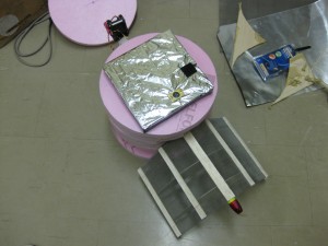
T minus 32400
We will be launching the IRIS II capsule shortly after noon today. It’s too hard to arrange to have everyone to drive out on such short notice, but we’ll definitely be making a post-mission post! Stay tuned! :o)
Edit: Launch was canceled today
Design Project Symposium
Posted by Scott Kuo in Presentations on March 22, 2010
The 10th annual ECE Design Project Symposium is coming up this Wednesday in the Davis Centre at University of Waterloo from 9:30 AM to 8:00 PM. The Project IRIS team will be there to demonstrate our capsule to the public. In addition to Project IRIS, there will also be many other innovative ECE student projects this year, such as a multi-touch screen, 3D drawing technology, a CVT bike and many many more!
Come look for us in the main lobby area in front of the DC library on Wednesday; you can’t miss us! ;)
2010 Ontario Engineering Competition
Posted by Alex Fefer in Presentations on February 1, 2010
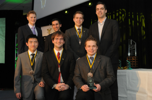
I’m extremely happy to announce that Project IRIS received 3rd prize in the Innovative Design category for the 2010 Ontario Engineering Competition! We had a great time participating and we’d especially like to congratulate the teams from the University of Ottawa and the University of Toronto who received 1st and 2nd prize respectively. All of the participating teams brought some truly innovative designs to the competition. Also, hats off to the OEC organizing committee at UW for a job well done.
New Concept Renderings
Posted by Alex Fefer in Engineering on January 23, 2010
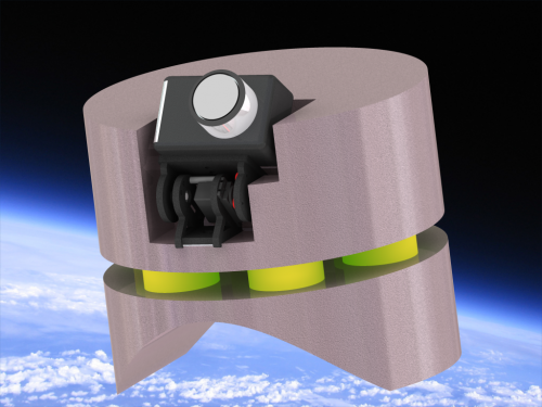
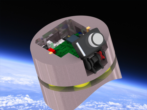
Since we finished modeling the new capsule just a few days ago, it was impossible to resist making a couple of renderings. :)
Here’s two shots, one with the cover (as it would appear in flight), and one without the cover so you can see what the inside of the capsule will look like.
Talking to the camera
Posted by Alex Fefer in Engineering on January 23, 2010
One of the best things about designing hardware yourself is that you have full control over exactly what you want the devices to do. Lately we’ve been figuring out what to do with the one piece of complex hardware that we didn’t design – the Canon SX100IS digital camera. Let’s just say that Canon’s engineers never imagined that anyone would be controlling the camera remotely from a normal PC, let alone an embedded board within a capsule that’s going up into the edge of the atmosphere.. Lucky for us, there’s a really dedicated group of Canon camera hackers out there that run an open-source project called CHDK, which sits on top of the Canon camera firmware and executes scripts that you write beforehand. These scripts can do a lot more than what you can normally access on the camera’s front panel. For instance, you can write a script to take pictures at certain intervals, choose flash settings, ISO, shutter speed, monitor the battery voltage – basically anything you want.
It sounds amazing, but the only problem with the CHDK is it still expects users to be able to press buttons on the camera and turn the scripts on and off! Obviously up at 100,000 feet there’s not going to be a human up there to press buttons, so we need some way to get our flight computer to talk to the camera. Unfortunately the camera won’t accept commands over the USB cable (we were hoping the CHDK would support this, but unfortunately it doesn’t). The other option, ripping off all the buttons on the camera and soldering wires connected to GPIO pins on our board, requires a lot of work to implement and means that we have to physically program in the button presses that correspond to the right menu options. Not fun. So we found a third solution…
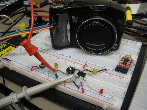
There’s a function you can call from within the scripts called get_usb_power. Interestingly, it returns how long (in ms) power was applied to the USB port on the camera. Now, even though we can’t actually communicate over USB, there’s nothing stopping us from sending bursts of “power” on the Vcc line over the USB cable… and transmit data as a sort of “morse code” based on the pulse length! Old-fashioned, sure – but it works, and it’s elegant enough that it doesn’t require us to do things like dismantle the camera and solder wires to every button on the camera’s front panel. So to test this, we threw together a quick circuit with the trusty 555 timer chip to generate pulses which we’ll send to the camera:
It goes to show that no matter what, there’s always some way to get a message through, even if it means using the USB power wire as a serial data cable. :)
Updates from beyond
Posted by Miron Vranjes in Engineering on January 15, 2010
The Project IRIS team has been hard at work redesigning the original capsule (IRIS I) in preparation for launch. The new design process has heavily utilized CAD visualization in order to minimize the amount of time spent creating and testing physical mock-ups. We are pleased to be able to show you a small preview of our latest design for your viewing pleasure.
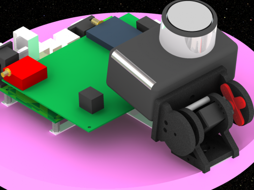
Newly designed IRIS II capsule as visualized in CAD software
Flight Control Unit
Posted by Alex Fefer in Engineering on July 25, 2009
We’ve been insanely busy over the last couple of weeks getting everything together, so we haven’t really had much of a chance to update the website and let you guys know what our electronics design is all about.
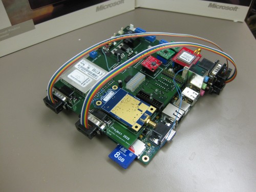
Our electronics package (which we call the FCU, or “flight control unit”) consists of two circuit boards. First is the Orchid/Colibiri carrier board, which we purchased from Toradex and contains the main CPU, memory, Ethernet controller, USB, and other “standard” peripherals. Naturally, this board doesn’t come equipped with the “nonstandard” instrumentation needed by Project IRIS: the 900MHz long-range UHF modem, GPS, GSM cellular module, accelerometers, magnetic compass module, barometric pressure sensor and so forth. We had to design our own daughterboard, which would sit on top of the carrier board to make an electronics “sandwich” of sorts.
A few weeks back, we created the circuit schematics using the EAGLE layout software, which contains thousands of libraries for standard components and also the physical “footprint” of each electronic part to assist us in designing the actual printed circuit board (PCB). After a few weeks of design, our fully laid-out PCB looked something like this (you get a prize if you can spot the errors!):
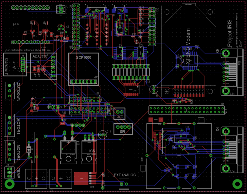
This is a two-layer PCB with a minimum trace width of 7 mils (0.007″), which is the smallest feature that can be produced by our circuit board manufacturer, AP Circuits. We can’t recommend these guys enough – we got our board back in 2 business days, complete with solder mask, legend layers, HASL (hot-air solder leveling – a special process to pre-coat all the exposed pads with solder), and not a single manufacturing defect that we could find. After another week of soldering and re-work to fix our design errors (if you look closely, you can see some small wires on on the board to take care of some mistakes we made in the initial prototype design), we selectively powered up each component and made sure everything worked. Click on the below image to see a 3D Photosynth of the complete FCU assembly with the two circuit boards mated together:
You might be wondering about the ribbon cables going across the top of the board; we’re using a few serial devices (the GSM, GPS and UHF modules), and to make development/debugging easier, we decided to keep the DB9 serial connectors so we could plug a computer into our board and interface with those components directly from a PC.
We’re now starting to think about our second revision of the board, which will be in design shortly to get rid of the design errors in the initial prototype.
Mechanical Construction
Posted by Scott Kuo in Engineering on July 25, 2009
A Photosynth of the Atmospheric Reconnaissance Capsule prior to the final application of radiation-reflecting Mylar material. (Click on image to view in 3D)
It is kind of difficult to have an idea of what is going on with all those pieces glued in, but we conveniently have a CAD drawing showing how the main body pieces together to provide a rigid lifting platform. :)
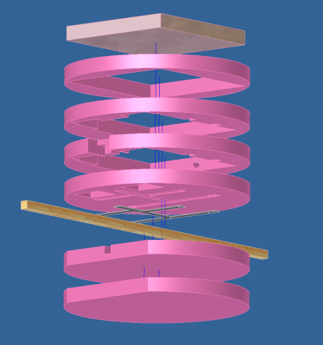
Showing off the guts
Posted by Scott Kuo in Engineering on July 18, 2009
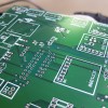
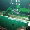
As of Friday afternoon, all of the components have finally made it to the Project IRIS team after hunting down on some MIA packages with Canada Post and UPS. So here’s a small collection of photos that we have taken over the past few weeks of some of our components.
(Click on thumbnail to open; use arrow keys to navigate)
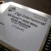
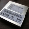
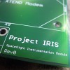
More to come…
Antenna Testing
Posted by Scott Kuo in Engineering on July 15, 2009
It’s been a while since we posted anything on the website because we’ve been working hard to put all of our components together. Here’s a video of us testing our parabolic dipole antenna that we are going to be mounting aboard the first assembly! This design gave us about a 9 dB gain when we tested over a more reasonable distance on campus. :)

